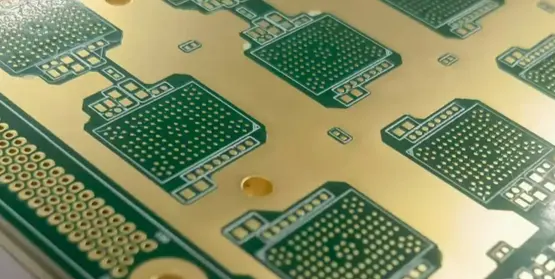
HDI PCB Manufacturing Services

High-Quality & Reliable PCBs of Benlida

Our HDI PCBs enable smaller, faster, and more reliable devices, making them essential for smartphones, wearables, medical equipment, and high-speed applications. Trust Benlida for precise multilayer PCB fabrication with fast turnaround and exceptional quality.

What is an HDI PCB?

A High-Density Interconnect (HDI) PCB is a type of printed circuit board designed with a higher wiring density per unit area than standard PCBs. HDI PCBs use microvias, blind/buried vias, and finer lines and spaces to pack more circuitry into a smaller footprint, enabling advanced electronic designs.

Difference from Standard PCBs

Standard PCBs typically have through-hole vias and wider traces, which limit the number of components and signal paths.HDI PCBs feature microvias and higher layer counts, allowing for more complex circuits in compact spaces.HDI boards support faster signal transmission, making them ideal for high-speed, high-frequency applications.

Benefits of HDI PCBs

Miniaturization: Supports smaller, lighter, and thinner devices.High-Speed Performance: Reduced signal loss and interference for high-frequency circuits.Higher Component Density: Allows more components per board, enabling multifunctional and advanced designs.Improved Reliability: Shorter interconnects reduce power loss and enhance thermal management.

HDI PCB Types

HDI PCBs come in several specialized designs to meet different performance and space requirements. Each type—Microvia HDI, Via-in-Pad HDI, and Blind/Buried Via HDI—offers unique advantages for miniaturization, signal integrity, and high-density component placement. Understanding these types helps designers choose the right HDI PCB for their advanced electronic applications.

Microvia HDI PCB

Microvia HDI PCBs use tiny laser-drilled vias to connect adjacent layers, allowing for high-density routing in compact spaces. They are ideal for smartphones, tablets, wearables, and other miniaturized electronics.

Via-in-Pad HDI PCB

Via-in-Pad HDI PCBs place vias directly beneath component pads, reducing signal path length and improving electrical performance. This type is commonly used in high-speed devices and BGA (Ball Grid Array) assemblies.

Blind/Buried Via HDI PCB

Blind and buried via HDIs connect specific inner layers without going through the entire board, enabling complex multilayer designs and often used in aerospace, medical, and high-performance computing applications.

HDI PCB Manufacturing Process

The HDI PCB manufacturing process combines precision engineering and advanced technology to produce high-density, high-performance boards. From material selection and microvia drilling to multilayer lamination and rigorous testing, every step is optimized to ensure reliability, signal integrity, and compact design for modern electronics.

Material Preparation

Choose the right substrate—FR-4, Rogers, or high-performance laminates—for reliable HDI PCB performance.

Microvia Drilling & Plating

Form microvias with laser or mechanical drilling, then plate for strong interlayer connections.

Layer Stackup & Lamination

HDI PCBs use 4–12+ layers, laminated precisely for high-density, high-speed designs.

Surface Finish Options

Protect and solder easily with ENIG, OSP, or HASL finishes.

Testing & Quality Control

Ensure reliability with electrical tests, AOI, and X-ray inspection.

HDI PCB Design Guidelines

Effective HDI PCB design ensures high-density, high-speed, and reliable circuits. Following best practices for trace width, via placement, layer stack, and signal integrity helps maximize performance and manufacturability.

Trace Width & Spacing Considerations

Maintain precise trace width and spacing to handle current, reduce crosstalk, and ensure reliable high-density routing.

Via Design & Placement

Optimize via type, size, and location for compact layout, signal integrity, and easy assembly.

Layer Stack Optimization

Plan the layer stack for signal performance, thermal management, and mechanical strength.

Signal Integrity & High-Speed Performance

Design for minimal interference and fast signal transmission in high-speed circuits

Why Choose Us for Multilayer PCB Manufacturing?

Quality Assurance

 BENLIDAPCBA guarantees superiorproduct quality by sourcinghigh-grade raw materials,adhering to internationallycertified quality managementsystems, and implementing arigorous six-stage inspectionprocess to proactively preventdefects

Competitive Prices

Maintaining in-housemanufacturing facilities grantsus direct oversight over bothquality standards andproduction expendituresFurthermore, our establishednetwork of dependablesuppliers provides certifiedmaterials at competitive pricing.

Fast Delivery

 BENLIDAPCBA  have 8 high-speed SMTmating lines, Daily productioncapacity exceeds 30 millionpoints.we can quickly completethe customer’s order.

Thoughtful Service

24-hour rapid response toprovide you with one-on-onenanny consultant pre-sales,sales, after-sales trackingservice, for you to answer anydifficult questions.

Typical Applications of HDI PCB

Benlida provides high-quality PCB manufacturing solutions for a wide range of industries.

From consumer electronics and industrial automation to medical, automotive, telecommunications, and aerospace applications, our PCBs are designed to meet the unique performance, reliability, and compliance requirements of each sector.

consumer pcb

Consumer electronics

Benlida manufactures reliable PCBs for smartphones, wearables, and other consumer devices, ensuring high performance.
industry pcb

Industrial automation

We provide durable PCBs for industrial machinery and control systems, supporting precision, efficiency, and long-term operation.
medical

Medical devices

Our PCBs meet strict safety and reliability standards for medical equipment, enabling accurate diagnostics and patient care.
auto pcb

Automotive electronics

Benlida produces high-quality PCBs for automotive systems, including infotainment, sensors, and control modules.
communicate

Telecommunications

We deliver PCBs for networking and communication devices, ensuring fast data transmission and reliable connectivity.
aero

Aerospace electronics

Our aerospace-grade PCBs are designed for extreme environments, providing high reliability for avionics and critical electronic systems.

Why Benlida is the Trusted HDI PCB Manufacturer

Quality Assurance

 BENLIDAPCBA guarantees superiorproduct quality by sourcinghigh-grade raw materials,adhering to internationallycertified quality managementsystems, and implementing arigorous six-stage inspectionprocess to proactively preventdefects

Competitive Prices

Maintaining in-housemanufacturing facilities grantsus direct oversight over bothquality standards andproduction expendituresFurthermore, our establishednetwork of dependablesuppliers provides certifiedmaterials at competitive pricing.

Fast Delivery

 BENLIDAPCBA  have 8 high-speed SMTmating lines, Daily productioncapacity exceeds 30 millionpoints.we can quickly completethe customer’s order.

Thoughtful Service

24-hour rapid response toprovide you with one-on-onenanny consultant pre-sales,sales, after-sales trackingservice, for you to answer anydifficult questions.

Request a HDI PCB Quote

Getting your HDI PCB project into production is simple with our easy and fast quote process. By submitting your Gerber files, BOM, and project details, our team can quickly evaluate your requirements and provide a clear, competitive quote.

Whether you need prototype assembly, low-volume production, or high-volume turnkey solutions, our streamlined RFQ process ensures fast feedback, accurate pricing, and guidance to optimize your PCB assembly for cost, quality, and lead time. Start your project with confidence and get your PCBs manufactured without delays.

Scroll to Top