Multilayer PCB Manufacturing Services
High-Quality & Reliable PCBs of Benlida
At Benlida, we provide high-quality multilayer PCB manufacturing services with fast-turn prototyping and reliable production. As a trusted multilayer PCB manufacturer, we deliver precision, efficiency, and one-stop PCB solutions for your electronic designs.
What is a Multilayer PCB?
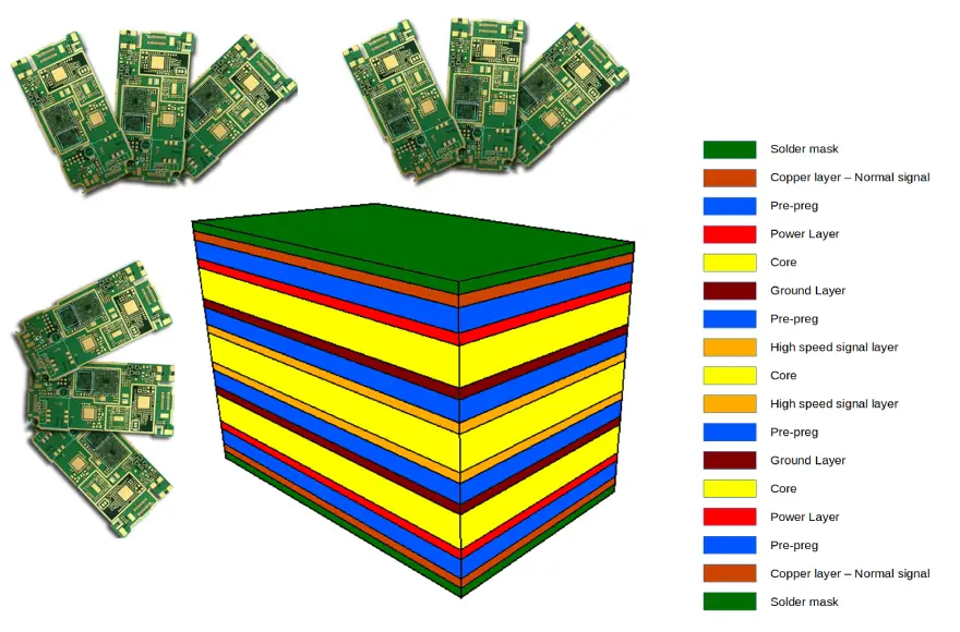
Printed Circuit Boards (PCBs) are the fundamental building blocks of all electronic devices. At Benlidapcba, we specialize in manufacturing three or more conductive layers PCBs, created by laminating single-sided and double-sided boards together with insulating materials (dielectrics) to form complex three-dimensional circuit structures.
From the outside, multilayer PCBs appear similar to double-sided boards on the top and bottom layers, but they contain additional internal layers on both sides of the core. Active and passive components are typically mounted on the outer layers, while the inner stacked layers are dedicated to routing and power distribution.
Our Multilayer PCB Manufacturing Services
Our multilayer PCB manufacturing services cover everything from rapid prototyping to full-scale production. With advanced technology and strict quality control, we deliver reliable, high-performance PCBs tailored to your design needs.
Our Multilayer PCB Manufacturing Process
The FR-4 PCB manufacturing process involves several precise steps to transform raw laminate materials into functional circuit boards. These steps include circuit imaging, etching, lamination, drilling, and surface finishing, all of which ensure the board meets the required electrical performance, reliability, and quality standards.
Material Preparation
The process starts with selecting and preparing FR-4 laminates and copper foils as the base materials for the PCB.
Inner Layer Imaging & Etching
Inner copper layers are patterned using photolithography and etched to form the circuit traces.
Lamination
Multiple layers are stacked and bonded under heat and pressure to create a solid, multilayer PCB structure.
Drilling & Plating
Holes and vias are drilled and plated to provide electrical connections between layers.
Outer Layer Imaging & Etching
A protective solder mask is applied, and surface finishes are added to protect the copper and ensure solderability.
Solder Mask & Surface Finish
A protective solder mask is applied, and surface finishes are added to protect the copper and ensure solderability.
Multilayer PCB Design Guidelines
In a typical four-layer stack-up at Benlidapcba, to improve electromagnetic compatibility (EMC) performance, signal layers should be positioned as close as possible to the plane layers. The tight coupling between signal traces and the ground plane reduces plane impedance, which further reduces common-mode radiation from cables connected to the PCB while decreasing crosstalk between traces.
Layer Function Assignment
In multilayer PCB design, the assignment of layer functions is crucial:
- Ground Plane: Typically dedicated to an entire layer, placed close to the top layer, providing excellent signal reference and EMI shielding
- Power Plane: Located in the middle of the board, powering the entire circuit and reducing power impedance
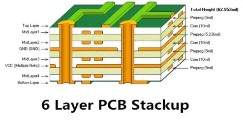
- Signal Layers: Remaining layers are used for signal routing. For example, in a six-layer board, there may be four signal routing layers and two power layers
A carefully designed multilayer PCB substrate can effectively reduce electromagnetic emissions and crosstalk while improving signal integrity and providing low-inductance power. Benlidapcba engineering teams design boards that increase immunity to RF fields by a factor of 10 or more compared to double-sided boards.
Power and Thermal Management
Copper traces on PCBs allow current to flow but also have resistance, which can alter current quality. Benlidapcba recommends:
- Controlled impedance traces for high-speed signals
- Increased copper thickness for power delivery networks
- Wider trace widths to control temperature rise
- Dedicated power/ground planes to reduce impedance
Multilayer PCB vs Other PCB Types
The FR-4 PCB manufacturing process involves several precise steps to transform raw laminate materials into functional circuit boards. These steps include circuit imaging, etching, lamination, drilling, and surface finishing, all of which ensure the board meets the required electrical performance, reliability, and quality standards.
| Feature / PCB Type | Single-Layer PCB | Double-Layer PCB | Multilayer PCB |
|---|---|---|---|
| Number of Layers | 1 layer | 2 layers | 3 or more layers (commonly 4, 6, 8+) |
| Design Complexity | Simple circuits | Moderate complexity | High complexity, supports dense circuitry |
| Signal Integrity | Basic, suitable for low-frequency | Improved, better for moderate signals | Excellent, ideal for high-speed and high-frequency circuits |
| Size & Density | Larger board for same circuit | More compact than single-layer | Highly compact, maximizes space |
| Cost | Low | Moderate | Higher, depends on layer count and complexity |
| Typical Applications | Simple electronics, toys, calculators | Consumer electronics, automotive, small appliances | Smartphones, computers, medical devices, aerospace, industrial electronics |
| Manufacturing Difficulty | Easy | Moderate | Complex, requires precise layer alignment and advanced techniques |
Why Choose Us for Multilayer PCB Manufacturing?
Quality Assurance
BENLIDAPCBA guarantees superiorproduct quality by sourcinghigh-grade raw materials,adhering to internationallycertified quality managementsystems, and implementing arigorous six-stage inspectionprocess to proactively preventdefects
Competitive Prices
Maintaining in-housemanufacturing facilities grantsus direct oversight over bothquality standards andproduction expendituresFurthermore, our establishednetwork of dependablesuppliers provides certifiedmaterials at competitive pricing.
Fast Delivery
BENLIDAPCBA have 8 high-speed SMTmating lines, Daily productioncapacity exceeds 30 millionpoints.we can quickly completethe customer’s order.
Thoughtful Service
24-hour rapid response toprovide you with one-on-onenanny consultant pre-sales,sales, after-sales trackingservice, for you to answer anydifficult questions.
Multilayer PCB Stackup & Thickness Options
The stackup and thickness of a multilayer PCB play a critical role in its performance, reliability, and manufacturability. Choosing the right layer count, board thickness, and material configuration ensures optimal signal integrity, thermal management, and suitability for high-speed or high-power applications.
Common Layer Counts
Multilayer PCBs typically start from 4 layers and can go up to 10 or more layers, depending on the circuit complexity. Common configurations include:
4-layer: Standard for moderate complexity circuits and compact designs.
6-layer: Offers better signal routing and improved power distribution.
8-layer and 10+ layers: Ideal for high-density boards, high-speed signals, and complex industrial or aerospace applications.
Standard vs Custom
Standard thicknesses: 1.6 mm is the most common, suitable for general applications. Other common options include 0.8 mm, 1.0 mm, and 2.0 mm.
Custom thicknesses: Available for specific mechanical, thermal, or high-frequency requirements. We can tailor the total board thickness by adjusting the number of prepreg and core layers to meet your design needs.
High-Speed or High-Power
High-speed circuits: Use controlled impedance stackups with dedicated ground and power planes to minimize signal loss and crosstalk. Thinner cores with precise layer spacing are preferred.
High-power applications: Thicker copper layers (2 oz or higher) and optimized stackups improve current carrying capacity and heat dissipation. Multi-layer designs help distribute power evenly across the board.
References & Sources
This guide is based on authoritative industry standards, academic research, and Benlidapcba technical documentation.
- Industry Standard
IPC-2221: Generic Standard on Printed Board Design
Institute for Printed Circuits (IPC), 2015.
→ View Standard - Research Paper
“High-Density Interconnect PCB Technologies for Mobile Devices”
IEEE Transactions on Components, Packaging and Manufacturing Technology, 2015.
→ View on IEEE Xplore - Academic Textbook
“High-Speed Digital Design: A Handbook of Black Magic”
Howard Johnson, Martin Graham, Prentice Hall, 1993.
ISBN: 978-0133957242
Contact Benlidapcba
For professional multilayer PCB manufacturing services, visit sterlingproductionmachining.com or contact our engineering team for design support and quotes.
Request a Multilayer PCB Quote
Getting your Multilayer PCB project into production is simple with our easy and fast quote process. By submitting your Gerber files, BOM, and project details, our team can quickly evaluate your requirements and provide a clear, competitive quote.
Whether you need prototype assembly, low-volume production, or high-volume turnkey solutions, our streamlined RFQ process ensures fast feedback, accurate pricing, and guidance to optimize your PCB assembly for cost, quality, and lead time. Start your project with confidence and get your PCBs manufactured without delays.