10 Key Design Practices to Optimize Your PCB Assembly Process
In today’s fast-paced electronics market, optimizing the PCB assembly process is essential for achieving high-quality products while minimizing costs and time-to-market. Whether you are a seasoned engineer or a newcomer to PCB design, understanding the best practices can significantly enhance your assembly efficiency. In this article, we will explore ten key design practices that will help you optimize your PCB assembly process.
1. Design for Manufacturability (DFM)
DFM is a set of principles aimed at simplifying the manufacturing process. By designing PCBs with manufacturing capabilities in mind, you can reduce potential errors and assembly time. Considerations include:
- Minimizing the number of layers
- Using standard components
- Avoiding tight tolerances where unnecessary
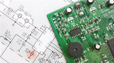
2. Schematic and Layout Optimization
Ensure that your schematic diagrams are clear and well-organized. This clarity extends to the PCB layout, where component placement can impact assembly efficiency. Key points include:
- Grouping related components
- Using design tools to check for errors
- Considering the assembly process when placing components
3. Component Selection
Choosing the right components can significantly affect the assembly process. When selecting components, consider:
- Availability and lead times
- Compatibility with assembly techniques (e.g., SMT vs. through-hole)
- Cost-effectiveness
4. Soldering Techniques
The soldering process is critical in PCB assembly. Understanding different soldering methods, such as reflow and wave soldering, can help you choose the right technique for your design. Some considerations include:
- Temperature profiles for reflow soldering
- Flux selection for different applications
- Minimizing thermal stress on components
5. Use of Test Points
Incorporating test points in your design allows for easier troubleshooting and quality control during the assembly process. This practice helps ensure:
- Efficient testing of electrical connections
- Quick identification of defects
- Improved reliability of the final product
6. Design for Assembly (DFA)
DFA principles focus on simplifying the assembly process itself. To implement DFA, consider:
- Reducing the number of parts
- Designing for easy handling and orientation of components
- Ensuring clear labeling on the PCB for assembly instructions
7. Simulation and Prototyping
Before moving to production, simulate your design and create prototypes to identify potential issues. Benefits include:
- Verifying circuit functionality
- Testing assembly processes
- Making necessary adjustments early in the design phase
8. Documentation and Standards
Proper documentation is essential for both the design and assembly processes. Standardizing your documentation practices can help ensure:
- Consistency across designs
- Clear communication with manufacturing teams
- Faster onboarding of new engineers
9. Collaboration with Manufacturers
Engage with your manufacturing partners early in the design process. This collaboration can lead to:
- Insights on manufacturability
- Identification of potential pitfalls
- Streamlined production flows
10. Continuous Improvement
Lastly, always strive for continuous improvement. Gather feedback from the assembly process and make iterative changes to your designs. Consider:
- Conducting regular reviews of assembly yields
- Incorporating lessons learned into future projects
- Staying updated with the latest PCB design technologies