Why HDI PCB for AI Applications is Changing the Tech Landscape
The global AI revolution is no longer just a software story; it is a hardware arms race. HDI (High-Density Interconnect) PCB technology is the essential infrastructure that makes modern AI applications possible.
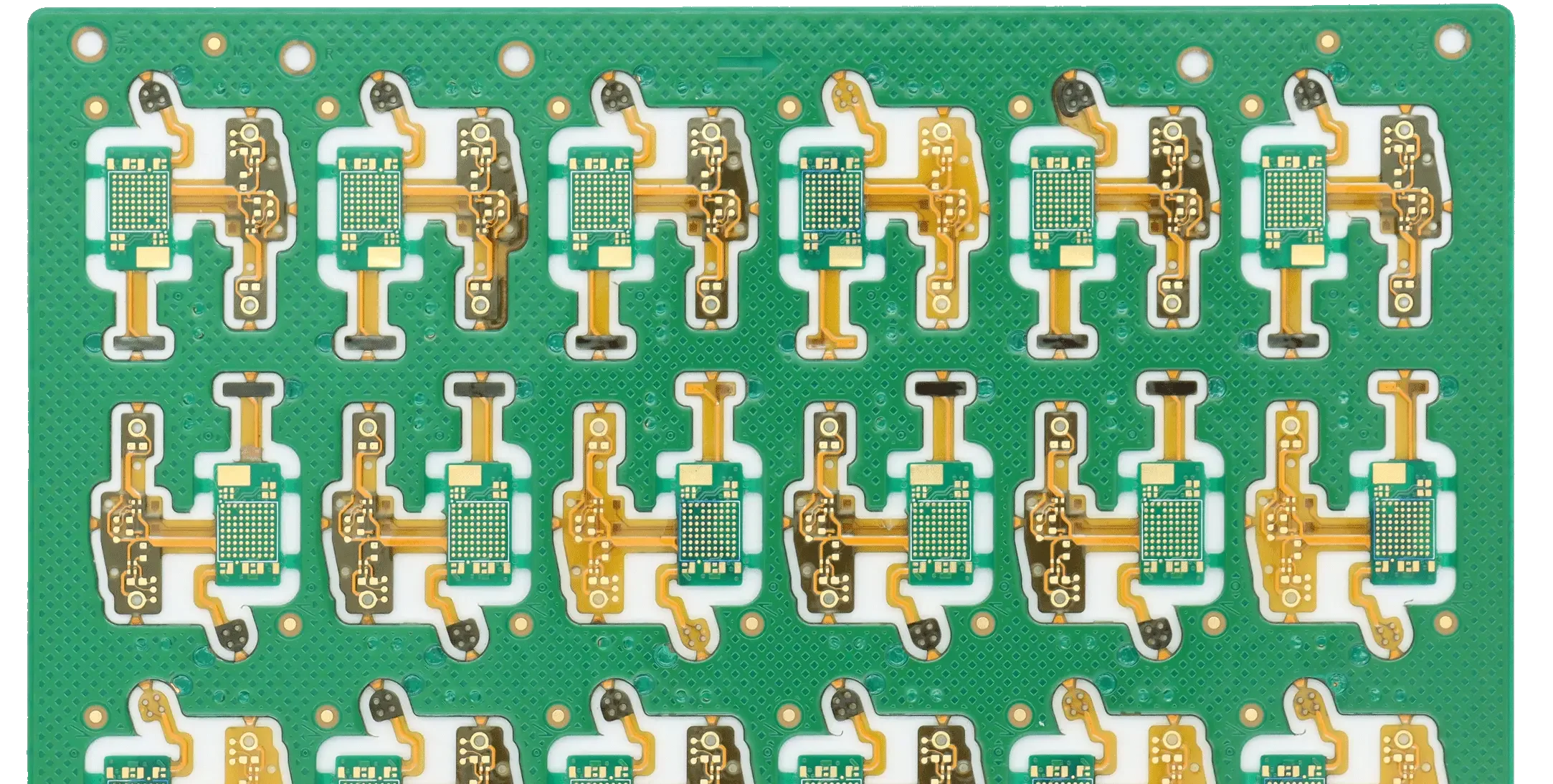
1. Understanding the Core: What is an HDI PCB?
Standard PCBs rely on mechanically drilled through-holes. In contrast, HDI uses laser-drilled microvias, allowing for much smaller connection points and significantly more routing space for high-speed AI processors.
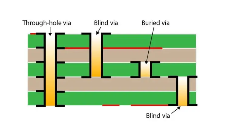
| Microvia vs Through-Hole: Technical Comparison | |||
|---|---|---|---|
| Specification | Traditional Through-Hole | HDI Microvia | AI Application Benefit |
| Via Diameter | 0.20 - 0.30mm | 0.075 - 0.10mm | 60% space savings for component placement |
| Layer Connection | Through entire board (stub effect) | Layer-to-layer only | No stub = 40% signal loss reduction |
| Routing Density | Standard density | 3x channels per layer | Supports 10,000+ pin BGA breakouts |
| Board Thickness | Limited by drill aspect ratio | Down to 0.4mm feasible | Enables AI edge device miniaturization |
| Impedance Control | ±10% tolerance | ±5% tolerance | Critical for 112G PAM4 signals |
| Signal Speed | Up to 10 Gbps | 112 Gbps PAM4 | PCIe 6.0 and beyond ready |
2. Industry-Specific Impacts
| Industry Segment | Key HDI Benefit | Critical Keyword |
|---|---|---|
| AI | Data Throughput | AI Server PCB |
| Automotive | Space Saving | Automotive PCBA |