Comparative PCB Design Strategies for Diverse Microcontroller Architectures
A comprehensive analysis of PCB design methodologies for AVR-Atmel, ARM-LPC, MSP, and Qwiic processor platforms.
Abstract
Modern embedded systems development requires navigating a complex landscape of microcontroller architectures, each presenting unique challenges for printed circuit board (PCB) design. This article presents a comprehensive comparative analysis of PCB design methodologies for four distinct processor platforms: AVR-Atmel (8-bit RISC), ARM-LPC (32-bit Cortex-M), MSP (Ultra-low-power 16-bit), and Qwiic (I2C-based modular ecosystem).
We examine critical design considerations including power distribution, signal integrity, thermal management, and design for manufacturability (DFM) specific to each architecture, providing engineers with actionable guidelines for optimizing their hardware implementations.
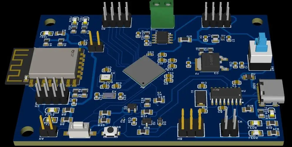
Introduction: The Architecture-PCB Design Nexus
The selection of a microcontroller fundamentally dictates PCB layout complexity, layer stack-up requirements, and peripheral integration strategies. While AVR-Atmel devices prioritize simplicity for hobbyist and low-power applications, ARM-LPC processors demand sophisticated high-speed routing techniques. MSP microcontrollers emphasize ultra-low-power PCB considerations, and the Qwiic ecosystem introduces standardized connector-based modularity.
The microcontroller will dictate the performance and capabilities of your design, so it's essential to consider several factors carefully before making a decision. Understanding these architectural constraints early in the design phase prevents costly revisions and ensures optimal hardware performance.
Architectural Characteristics
AVR microcontrollers utilize an 8-bit RISC architecture optimized for deterministic real-time control. Popular in Arduino ecosystems, these devices typically operate at clock speeds up to 20 MHz with straightforward pinout configurations, making them ideal for rapid prototyping and educational applications.
PCB Design Guidelines
| Design Parameter | Recommendation |
|---|---|
| Layer Count | 2-layer sufficient for most applications |
| Trace Width | 0.25mm standard, 0.5mm for power rails |
| Decoupling Capacitors | 100nF ceramic near VCC/GND pairs, 10µF bulk capacitor |
| Crystal Placement | Within 10mm of MCU, grounded guard ring for 16MHz+ crystals |
| Programming Interface | Standard 2x3 2.54mm ISP header at board edge |
Critical Layout Considerations
- Central Placement: Position the ATmega/Pmega device at the PCB's geometric center to minimize trace lengths to peripherals and reduce electromagnetic interference.
- Power Distribution: Implement star grounding for analog and digital sections when using ADC peripherals to maintain signal integrity.
- Thermal Management: Minimal requirements due to low power dissipation (<200mW typical), though thermal relief patterns recommended for ground plane connections to facilitate soldering.
Architectural Characteristics
ARM Cortex-M based LPC microcontrollers (NXP) deliver 32-bit processing power with clock speeds exceeding 100 MHz, requiring stringent high-speed design practices and controlled impedance routing for reliable operation.
Advanced PCB Requirements
Layer 2: Ground Plane (continuous, low impedance)
Layer 3: Power Plane (split analog/digital if required)
Bottom Layer: Signal (general purpose I/O)
// Minimum 4-layer stack-up recommended for 100MHz+ operation
Signal Integrity Protocols
For ARM-LPC designs, controlled impedance routing is mandatory to ensure reliable high-speed communication:
- USB/Ethernet Differential Pairs: Maintain 100Ω differential impedance with ±5% tolerance; route pairs with consistent spacing and minimize via transitions.
- Trace Geometry: Use 45-degree angles or curved traces; avoid right-angle turns that cause impedance discontinuities and signal reflections.
- Via Management: Maximum via aspect ratio of 0.8:1 for reliability; place vias near decoupling capacitors to reduce inductance in the power delivery network.
- Length Matching: Match high-speed trace lengths to within 25 mils to prevent timing skew in parallel bus configurations and differential pairs.
Power Distribution Network (PDN)
- Decoupling Strategy: Multi-tier approach with 0.1µF (high-frequency), 1µF (mid-frequency), and 10µF+ (bulk) capacitors per power domain to address wideband noise.
- Power Plane Resonance: Maintain plane separation of 3-5 mil dielectric thickness to minimize cavity resonance above 500 MHz and reduce EMI emissions.
Architectural Characteristics
Texas Instruments' MSP430/MSP432 families prioritize energy efficiency, with active currents as low as 100 µA/MHz and standby currents in the nanoampere range. PCB design must minimize leakage paths and parasitic power consumption to achieve datasheet specifications.
Power-Optimized PCB Strategies
| Critical Design Rule | Implementation |
|---|---|
| Leakage Prevention | Maintain >0.5mm clearance between high-voltage and low-voltage domains to prevent parasitic current paths |
| Battery Connections | Use wide copper pours (≥1mm) for battery terminals to minimize series resistance and voltage drop |
| Sleep Mode Considerations | Isolate always-on circuitry (RTC, backup domain) from main power rails using LDOs with <1µA quiescent current |
Specialized Layout Techniques
- Component Grouping: Cluster power-hungry peripherals away from the MSP core to enable aggressive power gating and domain isolation.
- Clock Distribution: Place 32.768 kHz crystal within 5mm of dedicated LFXT pins with matched load capacitors (12.5pF typical) to ensure stable real-time clock operation.
- Ground Plane Segmentation: Consider star grounding for systems with mixed analog sensors and digital processing to prevent ground loop interference.
Architectural Philosophy
SparkFun's Qwiic standard leverages 4-pin JST connectors (3.3V, GND, SDA, SCL) with integrated 2.2kΩ pull-up resistors, enabling rapid prototyping without soldering. This ecosystem prioritizes interoperability and reduced time-to-market over optimization.
PCB Integration Guidelines
│
├── Qwiic Port 1 (Primary I2C Bus) → Sensor Module A
├── Qwiic Port 2 (I2C Bus) → Sensor Module B
└── Qwiic Port 3 (Secondary I2C/Addressable) → Display Module
// Daisy-chain topology supports up to 3-4 modules at 400kHz
I2C Signal Integrity for Qwiic
- Bus Capacitance: Keep total trace capacitance <400pF (typically supports 3-4 modules at 400kHz); excessive capacitance degrades signal rise times.
- Pull-up Resistor Placement: Locate 2.2kΩ resistors on the master device only; remove duplicates on slave modules to prevent over-driving and excessive power consumption.
- Trace Routing: Route SDA and SCL in parallel with 0.5mm spacing; avoid crossing high-speed digital traces to minimize crosstalk and clock jitter.
- Address Conflicts: Implement I2C address selection jumpers (0Ω resistors) on PCB for module flexibility, allowing multiple identical sensors on the same bus.
Comparative PCB Design Matrix
The following matrix summarizes key PCB design parameters across all four architectures, enabling rapid technology selection based on project requirements:
| Feature | AVR-Atmel | ARM-LPC | MSP | Qwiic |
|---|---|---|---|---|
| Typical Layers | 2-4 | 4-8 | 2-4 | 2-4 |
| Min Trace Width | 0.2mm | 0.1mm | 0.25mm | 0.25mm |
| Impedance Control | Rarely required | Mandatory | Optional | Not required |
| Thermal Vias | Minimal | Extensive | Minimal | Minimal |
| Decoupling Strategy | Simple | Multi-tier | Ultra-low leakage | Standard |
| Programming Interface | ISP/SPI | SWD/JTAG | Spy-Bi-Wire/JTAG | USB/Serial |
| Manufacturing Cost | Low | High | Medium | Low-Medium |
Universal Design for Manufacturability (DFM) Principles
Regardless of processor selection, these practices ensure production success and minimize yield issues during scale-up:
Component Placement
- Align all polarized components (diodes, electrolytics) in uniform direction for automated assembly
- Maintain ≥0.5mm spacing between SMD components for pick-and-place tolerance
- Deploy 1.0mm diameter test points on critical nets (power rails, clock signals, reset lines)
Thermal Management
- Use 0.3mm diameter vias with 1.2mm pitch under power regulators and motor drivers
- Implement 2oz copper for power-intensive sections; standard 1oz for signal layers
- Ensure adequate copper area for heat dissipation in high-current paths
Documentation Standards
- Specify layer stack-up with exact dielectric thicknesses
- Define impedance control requirements with tolerance ranges
- Include embedded component specifications for advanced designs
Architecture-Driven Design Decisions
Effective PCB design for embedded systems requires deep understanding of the target microcontroller's electrical characteristics. AVR-Atmel designs benefit from simplicity and accessibility, while ARM-LPC implementations demand rigorous signal integrity engineering. MSP platforms require meticulous attention to power leakage paths, and Qwiic integration prioritizes standardized, modular connectivity.
By aligning PCB layout strategies with these architectural constraints—rather than applying generic rules—engineers achieve optimal performance, reliability, and manufacturability. The convergence of these diverse processor ecosystems ultimately enables more robust and scalable embedded hardware solutions.